TUESDAY, 29 SEPTEMBER 2020
Ever since the discovery of graphene in 2004, scientists have been rather excited by so-called '2D materials'. These materials, which are only one atom thick, have highly unusual electrical and mechanical properties when compared with their 3D counterparts. However, they have some practical limitations. It is very difficult to manufacture 2D materials without flaws because of how delicate the structure is. Additionally, for most macroscopic applications, you need more capacity than just a single layer can provide, for properties such as a higher conductivity or tensile strength. Several layers acting in parallel are desired, as opposed to a single layer, but sheets of atoms cannot simply be stacked or they will tend to return to a 3D material with none of the unusual properties.This is where the role of the 'hybrid superlattice' steps in. These unusual lattices allow us to aggregate several layers, increasing capacity, and yet the layers still conduct as if they were separated. The name might seem like it belongs in a 1980s sci-fi film but it does in fact describe the material very well; the structure is made up of individual, stacked-up sheets of a 2D material forming a 'superlattice', and between each sheet is a layer of an organic insulator (hence 'hybrid'). The key point is that the insulating layers do not allow conduction between the sheets so that they still act like individual 2D materials, preserving the unusual electronic properties. Flaws in individual sheets also become less of a problem due to the possibility of different manufacturing methods; scientists had previously tried separating the layers with alkali metal atoms (intercalation), but the conducting properties of the whole material were significantly changed. Here I explore the construction and exciting properties of this new class of material, looking in detail at a couple of examples that are attracting attention right now for their promise in technological applications.
Constructing the lattice
Hybrid superlattices can be constructed layer-by-layer through self-assembly, or by organic infiltration of an existing inorganic lattice to form the layered structure. The layer-by-layer technique is very precisely controlled; an inorganic gas is blown near the substrate with which it forms chemical bonds and a new layer. An inert gas is then added to remove the gas before the organic gas is inserted to do the same. This process is repeated, with the growth time of the inorganic layer carefully controlled to ensure the layer is of atomic thickness. The self-assembly approach is a bit messier - for certain combinations with the right electrostatic interactions, two suspensions of the organic and inorganic layers are mixed and will be attracted to each other to form a layered structure.
There is a third method, which is less common, involving small, organic molecules in solution diffusing into the inorganic lattice. A lot of the time, the energy needed to break the bonds in the inorganic lattice is more than the weak energy released when bonds formed with organic molecules. From a thermodynamic standpoint, since the process also involves an increase in entropy (the structure is becoming more ordered), in these cases the process cannot occur.
Transition metal dichalcogenides (TMDs) as ideal semiconductors
First up: transition metal dichalcogenides (TMDs). 2D layers of this material are layered with an organic matrix. The identity and thickness of the matrix depends on the application; for example, TMDs can be layered with porphyrin polymer to make a capacitor[4], since porphyrin has a good dielectric constant and the two layers can be made to bond strongly. The design will have a different capacitance depending on the thickness of porphyrin that you use. TMDs have the general formula MX2, where M is a transition metal atom and X is a chalcogen (group 16 on the periodic table) such as S, Se or Te.
The exciting thing about this family of compounds is that several of its members have unusually good semiconducting properties. A semiconductor is a material with special conducting capabilities, composed of a conductor and an insulator that is useful in electrical components like diodes and transistors. The unusual conducting properties arise due to the existence of a small energy difference, or 'band gap', between the 'valence band', the region of energy and space where electrons usually are confined to, and the higher energy 'conduction band', which allows electron movement throughout the structure. Electrons have a variety of energies, and usually because the band gap is only small, only a few will have enough energy to occupy the conduction band. At high temperatures or in bright light, electrons are given an energy boost so more can be 'excited' to the conduction band. These bands are not actually a continuous region of space and energy that electrons can occupy; they are a series of 'molecular orbitals' (MOs). Put simply, these are regions of space in a molecule that up to two electrons can occupy, which have an associated energy. The valence band and conduction band each contain lots of MOs that are very close in energy.
For an electron to move from the valence to conduction band, it is easiest to transition from the highest energy MO of the former to the lowest energy of the latter. However, there is a catch; momentum must be conserved in the transition, so the momentum of the MOs must match exactly. Otherwise, a vibration ('phonon') of the right momentum travelling from the rest of the lattice must happen to be incident on the electron, at the instant it collides with a photon to give it the energy to make the transition. These three-way collisions are highly unlikely, which is why most materials don't make good semiconductors. Unlike their 3D counterparts, 2D TMDs happen to have an exact momentum match, making them excellent semiconductors.
Why is all of this useful? The drive towards miniaturising electronics has left even the best silicon-based metal–oxide–semiconductor field-effect transistors[5] (MOSFETs) behind, with concerns that heat dissipation and quantum effects may become more significant at tiny length scales. Hybrid superlattices of TCMs, which still retain their semiconducting properties at any thickness, could provide a promising alternative.
MXenes for electromagnetic screening and water purification
Up next is MXenes. These are 2D layers in a hybrid superlattice with the structure Mn+1XnTx, where M is a transition metal, X is carbon or nitrogen and T is a functional group, like -OH, that can be incorporated to terminate the structure at the surface. These metal carbides have a slightly weird combination of both metallic and ceramic properties. The layers have amazing conducting abilities, so are promising as electrodes for lithium ion batteries or supercapacitors as they can sustain a high surface charge density. They are also very good at absorbing photons from the sun, so can be used to purify water through rapid evaporation using energy from only sunlight, at an 84%[6] efficiency. The reason they are better than metals at this is the T groups are hydrophilic, so water molecules cluster around the MXene membrane.
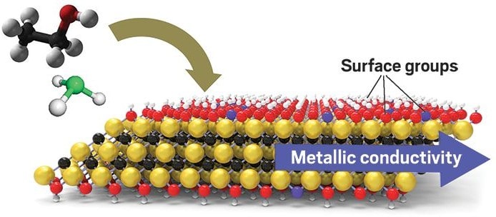
The crystal structure of a 2D layer of a MXene, showing hydrophilic surface groups. Extracted from https://pubs.acs.org/doi/abs/10.1021/acsnano.7b07460 with permission from the American Chemical Society.
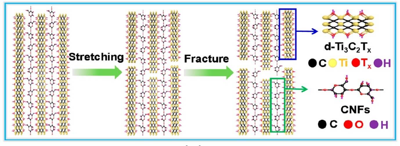
The crack-deflection mechanism in MXene hybrid superlattices. Extracted from https://pubs.acs.org/doi/pdf/10.1021/acsnano.8b00997 with permission from the American Chemical Society.
Pip Knight is a second year student from Churchill College studying Natural Sciences
References
- [BACK] Huang, Yujia, et al. Hybrid superlattices of two-dimensional materials and organics. Chemical Society Reviews (2020)
- [BACK] Wang, Qing Hua, et al. Electronics and optoelectronics of two-dimensional transition metal dichalcogenides. Nature Nanotechnology 7.11 (2012): 699-712.
- [BACK] Cao, Wen-Tao, et al. Binary strengthening and toughening of MXene/cellulose nanofiber composite paper with nacre-inspired structure and superior electromagnetic interference shielding properties. ACS Nano 12.5 (2018): 4583-4593.
- [BACK] Woodford, Chris. How do capacitors work? ExplainThatStuff, 23 Sept 2020
- [BACK] Woodford, Chris. How do transistors work?. ExplainThatStuff, 21 Sept 2020
- [BACK] Berger, Michael. What are MXenes? Nanowerk, 21 Sept 2020,https://www.nanowerk.com/mxene.php
- [BACK] Gobbi, Marco, et al. Collective molecular switching in hybrid superlattices for light-modulated two-dimensional electronics. Nature Communications 9.1 (2018): 1-9.
